- TOP
- Media
- ALCONIX's BluePrint
- Rewiring Society with Next‑Gen Power Semiconductors — How Novel Crystal Technology and ALCONIX Are Making the Future
Rewiring Society with Next‑Gen Power Semiconductors — How Novel Crystal Technology and ALCONIX Are Making the Future
Can a trading company be the partner that helps startups cross the “Valley of Death”?
Yet the road from invention to commercialization is full of hurdles. To mass‑produce and distribute a product or service at commercial scale, the supply chain—from procurement to manufacturing to logistics—must be designed and built. That means engaging the target market early, testing real demand, and establishing reliable, on‑time supply capabilities. This takes significant capital, talent, and time. Many startups struggle at this stage and ultimately halt operations, a phenomenon widely known as “Valley of Death.”By contrast, a trading company’s core business is to bridge gaps between supply and demand so that goods and services flow smoothly. With roots in international trade, trading companies combine logistics functions and deep market/industry know‑how to develop demand and coordinate supply networks—a solution set that is uniquely theirs.For startups, a trading company with commercialization know‑how can be a powerful partner in crossing the Valley of Death. Trading companies, in turn, gain the benefit of adding society‑changing solutions to their own portfolio.This is especially true in materials and manufacturing, where scaling up requires large‑scale equipment and steady supplies. Precisely because this domain is hard, ALCONIX, a materials trading company long embedded in manufacturing supply chains, has the experience to run alongside such startups and support them effectively.
What trading companies can do for startups building the future
The ALCONIX Group operates a corporate venture capital (CVC) fund to invest in startups. But it doesn’t stop at capital. ALCONIX also provides marketing and sales support in collaboration with its operating divisions, and conducts prototyping and contract manufacturing through group manufacturing companies.
According to Mr. Ueyama, Executive Officer of the Business Strategy Department, which runs the day‑to‑day of CVC operations:
“[ALCONIX launched its CVC] so as to discover and handle cutting‑edge products that had yet to reach the market, and to differentiate itself from competitors. […] when it comes to high‑novelty materials or technologies without adoption records, taking calculated risk to reach for future business—that, we felt, is the essence of business.”
See also our feature on ALCONIX’s CVC activities.
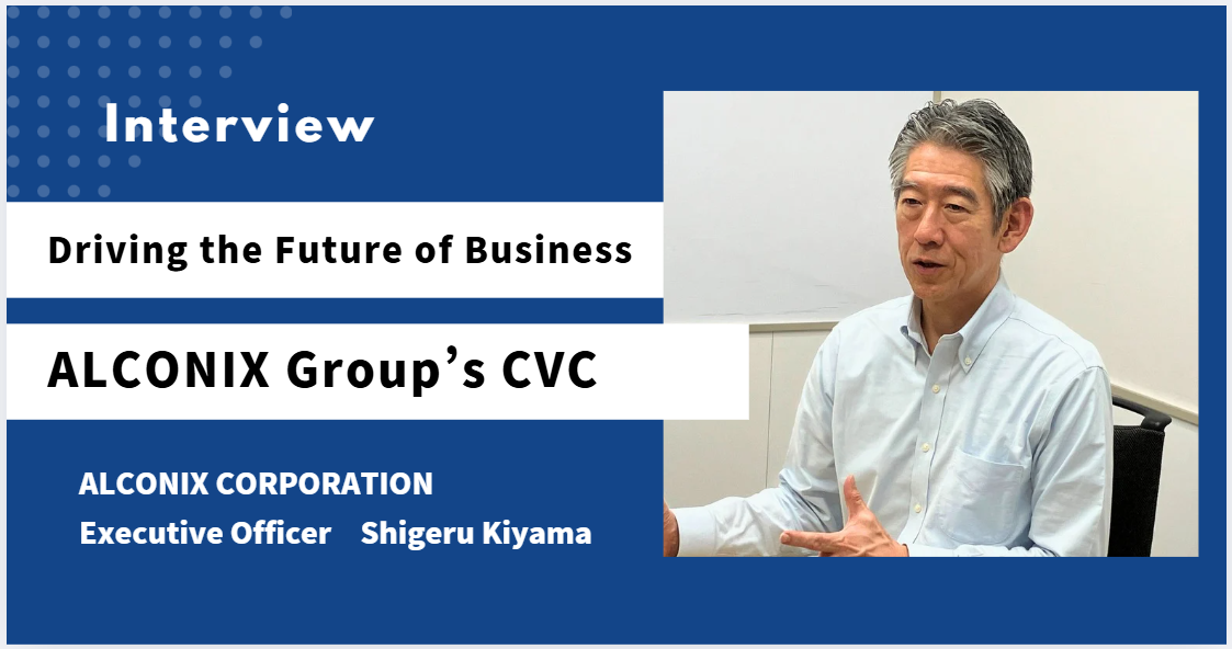
ALCONIX's Corporate Venture Capital: Driving the Future of Business
ALCONIX VENTURES CORPORATION. — official website.
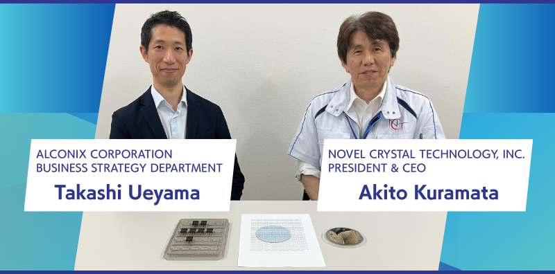
What, then, can a group rooted in trading actually do for its portfolio companies? We asked Mr. Akito Kuramata, President & CEO of Novel Crystal Technology, Inc. (NCT)—a startup developing and manufacturing β‑Gallium Oxide (β‑Ga₂O₃) wafers for next‑generation power semiconductors—and Mr. Ueyama from ALCONIX’s Business Strategy Department.Together, a materials startup and a materials trading company can catalyze meaningful change. Here is the BluePrint—the design for the future—the two leaders are drawing.* β‑Gallium Oxide is a compound made from the rare metal gallium. A wafer is the thin, disk‑shaped substrate on which semiconductor devices are fabricated.
From lab insight to a new company — founding Novel to turn gallium oxide into power devices
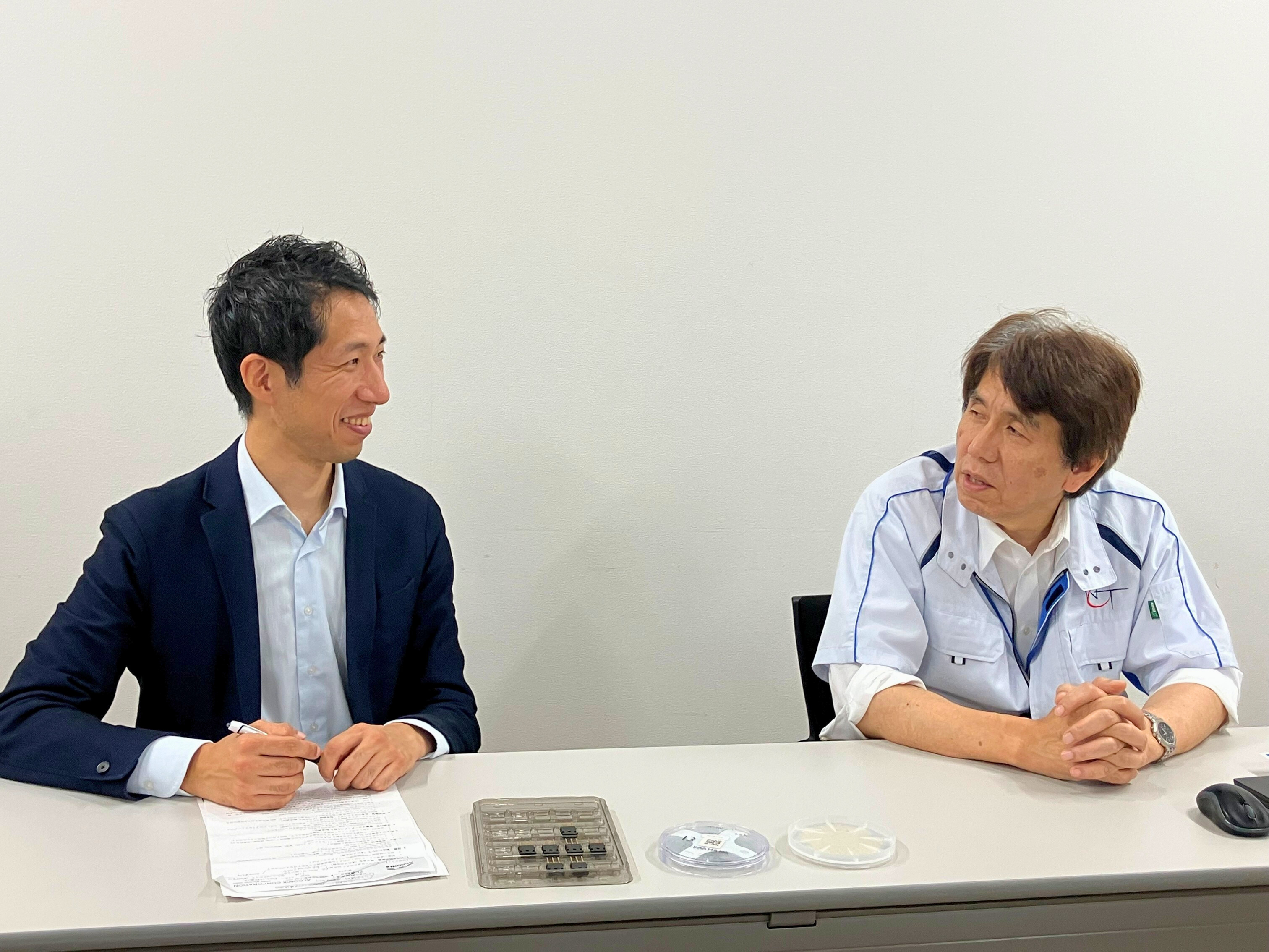
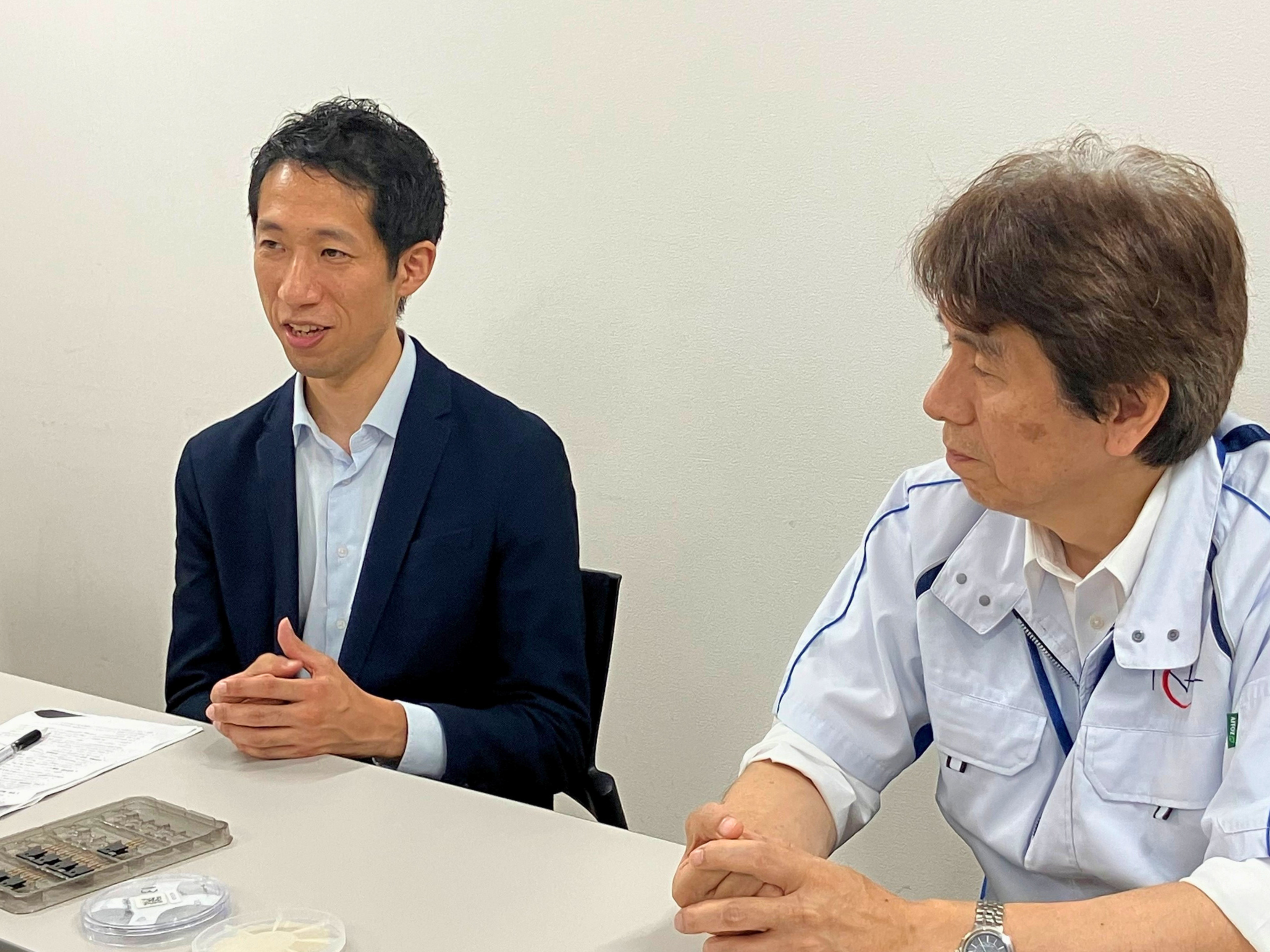
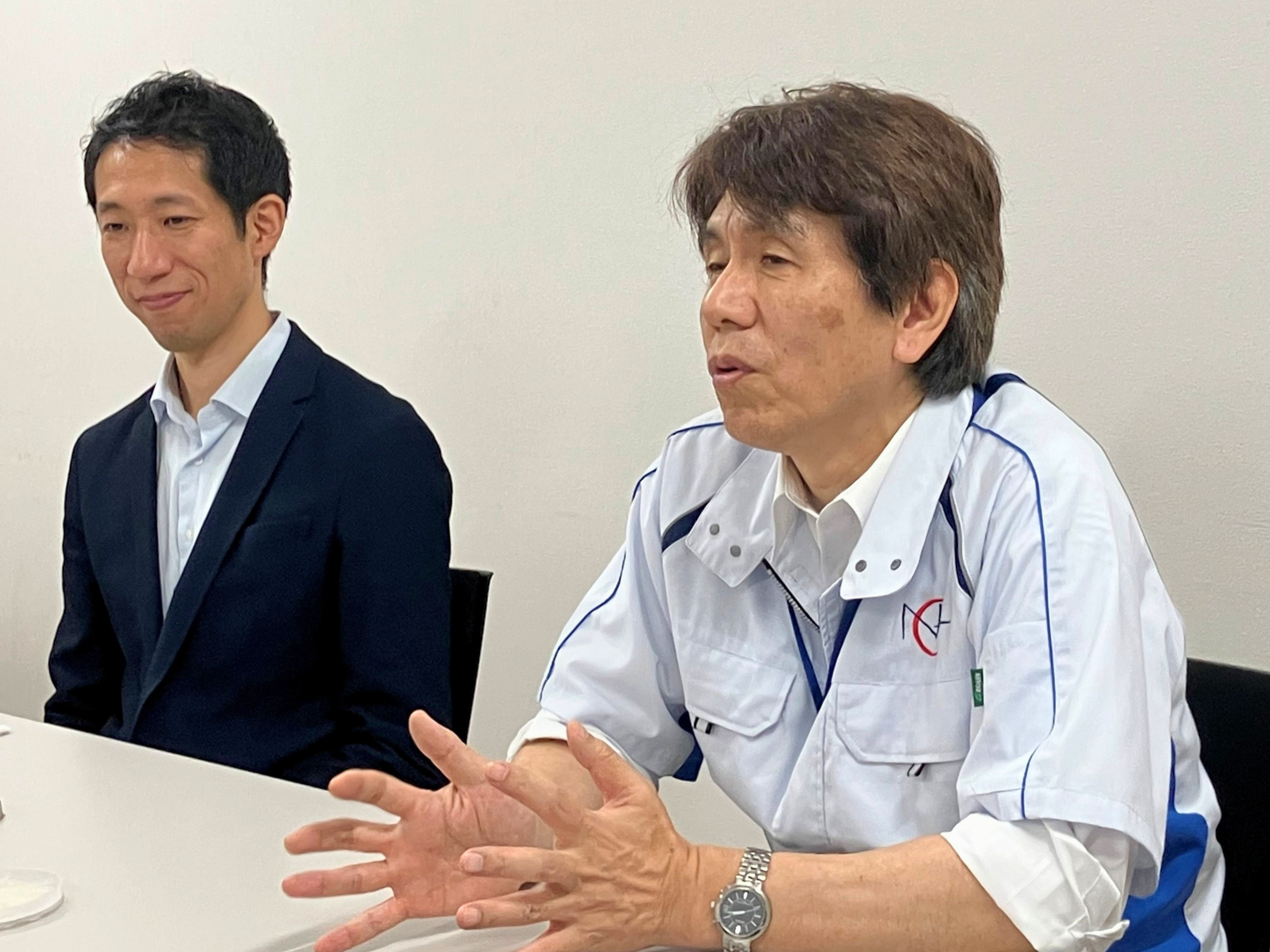
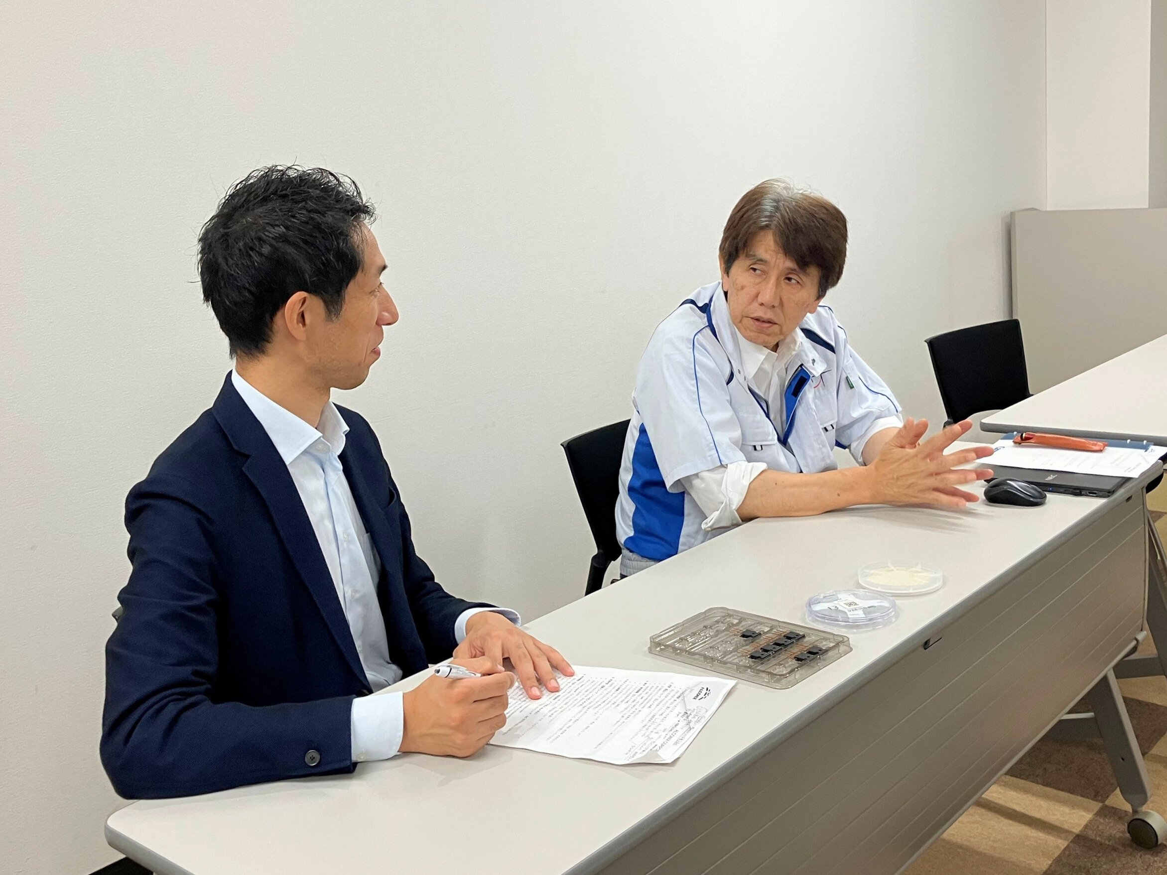
Ueyama (left) and President Kuramata (right)
Origins and founding story
President Kuramata:
β‑Gallium Oxide was initially researched at Tamura Corporation, an electronic components manufacturer that became the base of NCT, as a substrate for LEDs. I joined that team in 2008. As we proceeded, we wondered whether the transparent and conductive properties of β‑Ga₂O₃ could be applied elsewhere. Through Professor Shizuo Fujita at Kyoto University, I met Dr. Masataka Higashiwaki of NICT (National Institute of Information and Communications Technology), who was exploring transistor applications of β‑Ga₂O₃, and we began working together.
In 2011, we published a paper on our results. That helped spark a global movement toward developing power devices (power semiconductors) using β‑Ga₂O₃, and we started receiving many inquiries for research‑grade wafers.
At the same time, the LED substrate path that Tamura had prioritized became uneconomic around 2015 as competition from China intensified and alternative technologies emerged. We asked Tamura to invest in wafer manufacturing equipment for the power device route, but they judged it difficult to invest further in β‑Ga₂O₃ equipment given the LED business outlook.
After about a year of deliberation, we proposed a spin‑out and outside capital so that we could continue our work on power devices. Tamura’s CEO, from the founding family, strongly empathized with our desire to keep the research going—that support helped us establish Novel Crystal Technology.
I had long wanted to commercialize the technology I helped develop in a company I founded. Moving from researcher to manager comes with risk, and there was a real chance it wouldn’t work. But I felt, if I miss this window of opportunity, I might never get another, so I decided to go for it.
Why gallium oxide matters — device physics in plain terms
President Kuramata:
Semiconductors rectify current (AC/DC conversion), amplify signals, and switch current rapidly on and off. Power semiconductors use these capabilities to adjust frequency and voltage and supply power efficiently and stably.
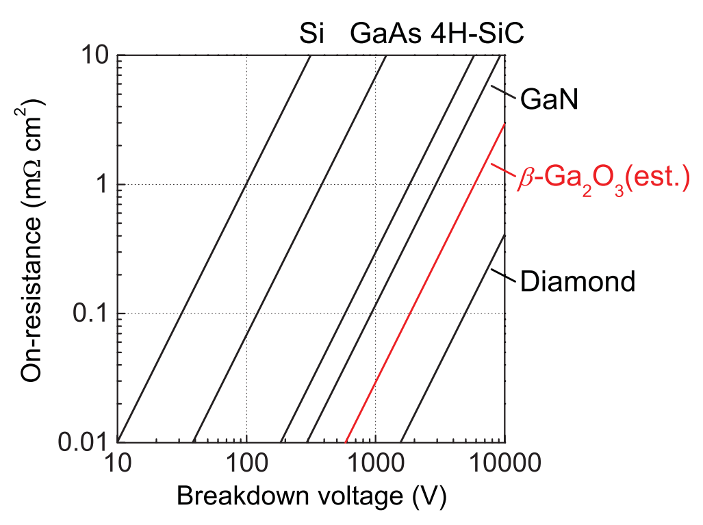
In a power device, there’s a layer called the drift layer that ensures high‑voltage tolerance. A thicker drift layer can withstand higher voltages but also increases resistance. Voltage tolerance correlates strongly with the material’s bandgap—a larger bandgap enables high voltage tolerance in a thinner layer. But a larger bandgap also tends to make current flow harder.
Silicon (Si), Silicon Carbide (SiC), and Gallium Nitride (GaN) are already widely used in traction motor control (rail, automotive) and power supplies. β‑Ga₂O₃ has an even larger bandgap but still allows current conduction—so it can process ultra‑high‑voltage, high‑power with lower loss, which makes it highly attractive for power devices.
(Original citation: Development of gallium oxide
power devices, Higashiwaki et al., 2013)
Building for scale — the hard problems and how Novel is tackling them
President Kuramata:
First, at the device level: β‑Ga₂O₃ is hard to make p‑type. Many electronic components rely on combining n‑type and p‑type semiconductors (*), so we’re exploring solutions such as varying dopants or combining p‑type layers made from other materials.
For wafers, semiconductor manufacturing typically reduces cost by fabricating many chips on a single wafer, so larger wafers are preferable. Our current targets are 6 inches and ideally 8 inches. β‑Ga₂O₃ also has lower thermal conductivity, and as wafers grow larger, heat buildup can cause warpage or cracking. We’re researching thinner wafers, including techniques adapted from silicon processing, to overcome those issues.
(*) Pure semiconductors conduct poorly. To enhance functionality, dopants (impurities) are introduced to create n‑type and p‑type semiconductors.

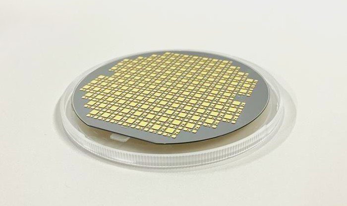
Transparent β‑Ga₂O₃ wafer
Epitaxial film deposited on a wafer — device fabrication starts from here
Investing to commercialize — ALCONIX and Novel’s division of roles
Why ALCONIX invested
Mr. Ueyama:
ALCONIX has a long track record handling compound semiconductor wafers, and I personally started paying close attention to β‑Ga₂O₃ around 2017. I knew it would take time to realize β‑Ga₂O₃ power semiconductors, but I wanted us to invest. The opportunity didn’t come quickly, but after our CVC launched in 2021 and got on track, NCT approached us.
In compound semiconductors, many players are large companies. As a materials trading company, we constantly ask how we can differentiatedly handle ‘materials of the future’ as real business. When a startup like NCT offered us a chance to invest, it was ideal for how we envisioned our CVC framework.
President Kuramata:
Our policy for shareholders was not pure financial investment—we wanted partners to help build the business with us. ALCONIX already had experience in wafer business and had cultivated customer relationships in Europe. We valued their connections and depth in adjacent businesses, which led us to accept their investment.
How collaboration works
President Kuramata:
Our products don’t drop straight into existing mass‑production lines. Manufacturers have optimized lines around current materials, and they can’t switch to β‑Ga₂O₃ overnight.
ALCONIX has long engaged in international wafer trading, so they have many connections at device makers. They introduce our products and R&D progress, encourage device research using β‑Ga₂O₃, and relay feedback from those engineers back to us so we can reflect it in our products. That’s already very helpful.”
Mr. Ueyama:
Our role is to do whatever it takes to create the market. That includes selling prototype wafers, loaning devices for trials, and other steps so manufacturers can budget for research. We also supply wafers to deposition tool makers to encourage equipment development—we’re engaging multiple sides to broaden the supply chain.
Concretely, together with our Electronics Materials Dept.1 and our European subsidiary, we co‑exhibited with NCT at local trade shows and introduced NCT to major European semiconductor companies.
NCT’s shareholder base includes only one financial VC—the rest are operating companies. Each brings something unique: polishing technologies for wafers, device know‑how, and more. Everyone is gathering to bring β‑Ga₂O₃ to market, and we’re one of them.
President Kuramata:
Recently, ALCONIX helped introduce us to a world‑leading wafer manufacturer they’ve known for years. The company’s CTO even joined our web meeting. Their view was essentially: ‘Commercial deployment of β‑Ga₂O₃ will take a bit more time, so let’s wait a little.’ Even so, we continue to stay in touch with them.
The road to impact — small breakthroughs, big outcomes
What breakthroughs are needed for social deployment?
Mr. Ueyama:
In manufacturing, unlike software, results don’t come from one big breakthrough alone. They’re the sum of many small breakthroughs across every process step.
President Kuramata:
Exactly. For us, it’s not that we need one spectacular breakthrough. If we keep steadily advancing the programs we’re on, we’ll reach socially deployable levels. For example, we’ve made major progress in technologies to grow large crystals at low cost. On the device side, we’re seeing advances that resolve previously problematic phenomena. If we maintain this pace, we think we can reach the goal within a few years.
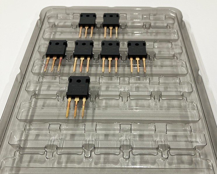
β‑Ga₂O₃ transistor samples — a glimpse of devices that may be embedded in future equipment
How commercialization of β‑Ga₂O₃ could change society
President Kuramata:
We expect much more efficient use of electricity. Because β‑Ga₂O₃ can handle ultra‑high‑voltage, high‑power, it will first be used in areas that deal with such electricity.
Renewables (solar, wind, etc.) are harder to use than nuclear or thermal today. Their voltage and frequency fluctuate, and generation sites tend to be far from demand centers. That can cause imbalances leading to blackouts, or curtailment (wasting potential output). Efficient use of renewables remains a challenge.
Japan is strengthening long‑distance HVDC (high‑voltage direct current) transmission to connect generation and demand across the country. Using β‑Ga₂O₃ power devices at ultra‑high voltage can make these systems far more efficient and lower‑loss. Likewise, grid‑balancing batteries can be charged more efficiently with lower losses. Taken together, β‑Ga₂O₃ will contribute to realizing a smart grid(*).
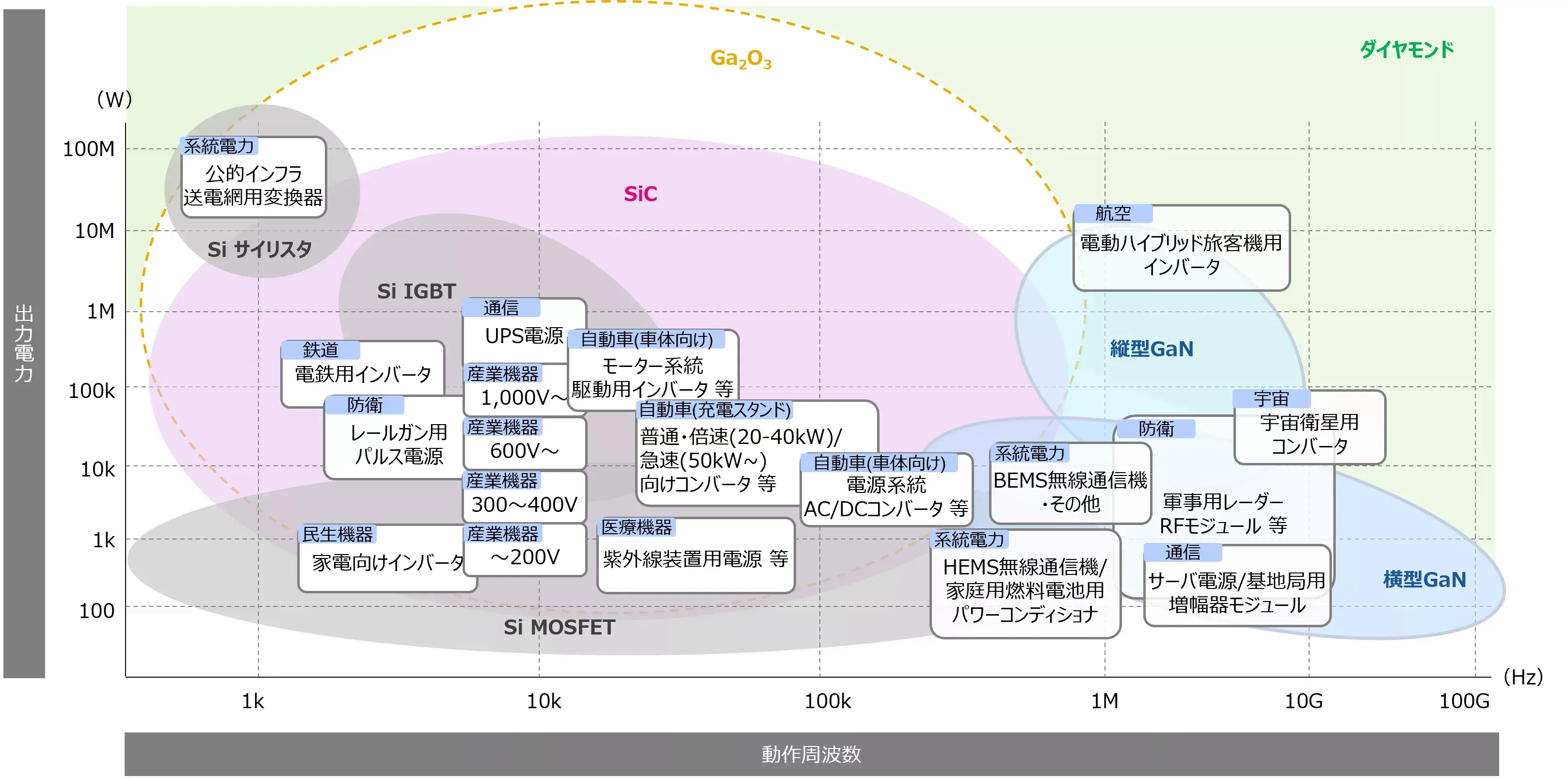
Chart (original source): パワー半導体 - KPMGジャパン(2023)(Power semiconductors by material — technology and application trends (KPMG Japan, 2023)).
*Smart grid: A next‑generation grid that uses ICT to monitor, control, and optimize power flows collaboratively between supply and demand, across all generation sources.
What NCT expects from ALCONIX to make this real
President Kuramata:
We want ALCONIX to work with us to implement new solutions and build the supply chain. Companies without experience can’t easily anticipate what will happen and how to proceed.
ALCONIX’s long experience in compound semiconductor business means we can consult them on next steps. Their customers likely feel the same, so we hope ALCONIX will keep positioning themselves between us and customers, and help align concepts and roadmaps.
Mr. Ueyama:
Thank you. In our trading segment we don’t own proprietary technology—our value is in gathering information and building commercial flows. That’s why, as we construct the supply chain, our sales teams keep their antennas up for what’s missing for product‑market fit, and we act as a bridge to fill those gaps.
Accelerate into the FUTURE — a growing market, unlocked by the power to connect
The power semiconductor market is forecast to double from approximately ¥3.5 trillion in FY2025 to around ¥7.7 trillion over the next decade. Most of that growth is expected to be driven by next‑generation power semiconductors—SiC, GaN, and potentially β‑Ga₂O₃, which may enter practical use around 2026.
(Original source: 「パワー半導体の世界市場を調査 | プレスリリース | 富士経済グループ」(Fuji Keizai Group press release on the global power semiconductor market.))
NCT and ALCONIX are tackling this growth market from both sides—materials development and commercial flow construction—to overcome barriers and deliver society‑changing innovation. In other words, it’s ALCONIX’s power to connect—linking seeds of research to diverse needs—coming into its own.
“Accelerate into the The FUTURE.” We are the watershed.